
Thin film integrated circuit components (MIC)
We provide integrated production of high grade alumina substrates for microwave applications from manufacturing to thin film pattern formation. From the initial prototype to mass production, we deliver high quality products at a low price over a short period of time.
Through hole & castellation
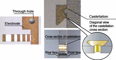
Through hole: By metalizing the inner wall of the through hole, the electric conduction of the top and bottom sides of the substrate can be achieved.
Castellation: By processing and metalizing a semicircle through hole on the side of the substrate, the electric conduction of the top and bottom sides of the substrate can be achieved.
Details
- Through-hole diameter: φ 0.1 to φ4
- Accuracy of position: ±0.02mm
Thin film capacitor
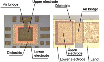
Dielectric material with small dielectric loss is sandwiched by the conductive electrodes. (upper electrode・lower electrode). The dielectric material can store electricity.
Details
- Dielectric material: SiO2(εr 4.2)
- Capacitance:
Standard specificiton: 103.4pF/mm2 (0.384μm dielectric film thickness) - Minimum dimension of dielectric: 0.1mm×0.1mm
(The electrode area that determines the capacitance value is smaller than the dielectric area.) - Withstand voltage: 30V or less (DC)
Lange coupler
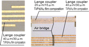
High-frequency signals can be distributed.Our Lange coupler enables manufacturing with line (20μm) and spacing (15μm). With the combination of "air bridge", the shortest wiring distance can be achieved.
Details
- Film composition
- Ti/Pd/Au
- Ti/Pt/Au
- Ti/Pd/Cu/Ni/Au
- Minimum line and space
Ti/Pd/Au , Ti/Pt/Au 20μm/15μm or more Ti/Pd/Cu/Ni/Au 30μm/20μm or more - Accuracy of pattern
Ti/Pd/Au , Ti/Pt/Au ±5μm (3μm Au plating thickness) Ti/Pd/Cu/Ni/Au ±5μm (1.5μm Au plating thickness)
Air Bridge
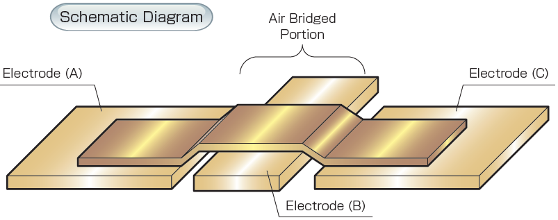
By using technology unique to JFC, if you use an air bridge that there is no need for wire bonding and the Inductance value can be reduced by the shortest connection distance.
Thin film resistor
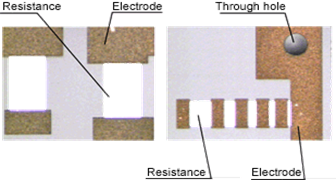
We use Ta2Nx, which is superior in environmental resistance, for the material of thin film resistors. The minimum line width is 20μm.
Details
- Material of resistor: Ta2Nx
- Sheet resistance value: 20Ω/□ , 50Ω/□ , 100Ω/□ , 130Ω/□
- Minimum line width of resistance: 20μm
- Temperature characteristic of resistance: -100±20ppm/℃
- Resistance tolerance: ±10%~ (Regarding tolerance, please consult us.)
Side pattern
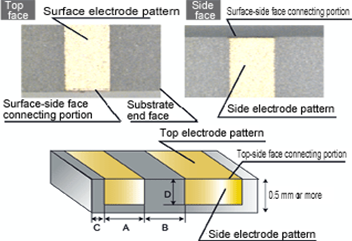
We can provide patterning to the side face.
For PD sub-mount and LD sub-mount, a side face metallize pattern is needed in order to establish a ground on the bottom face via the side face.
Details
- Applicable substrate thickness: 0.3mm or more
- Film composition: Ti/Pd/Au(3μm or more)
- Minimum pattern width for side face (A): 0.07mm±0.05mm
- Distance between side face patterns (B): 0.08mm or more
- Distance from the substrate end (C): 0.05mm or more(Regarding tolerance, please consult us.)
- Pattern length from the substrate end (D): 0.2mm or more ±0.1mm
Thin film inductor
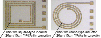
Inductor is a passive electronic component which stores electrical energy in the form of magnetism. Combining with the thin film capacitor, the LC circuits can be feasible.
Details
- Film composition
- Ti/Pd/Au
- Ti/Pt/Au
- Ti/Pd/Cu/Ni/Au
- Minimum line and space
Ti/Pd/Au , Ti/Pt/Au 20μm/15μm or more Ti/Pd/Cu/Ni/Au 30μm/20μm or more - Accuracy of pattern
Ti/Pd/Au , Ti/Pt/Au ±5μm (3μm Au plating thickness) Ti/Pd/Cu/Ni/Au ±5μm (1.5μm Au plating thickness)